This post will show how to use hardware overlays on our recently uploaded PYNQ system. We will add AXI interface software control for the onboard LEDs and push-button, as well a custom Verilog hardware module. This is a convenient way to interface hardware modules designed in hardware description languages (i.e. Verilog/VHDL) via an easy to use Python interface.
References:
[1] Creating and using hardware designs. Good intros to PYNQ overlays.[2] More details, including high performance interface and hierarchical hardware blocks.
[3] Adding ready-made IPs to PYNQ overlay.
Pre-requisites:
- Working Vivado installation. Vivado and version PYNQ versions should match and we installed PYNQ 2.5.x, so we use Vivado 2019.1.
- EBAZ4205 board with a booting PYNQ image.
2. AXI: this infrastructure provides a memory mapped interface for complex interaction of the PS with hardware modules (PL or physical IOs). These are banks of 32-bit registers that can be assigned to the processor memory in order to read and write hardware data. While the AXI interface is in fact very complex, we will use this simplified view as a starting point to present the concept and how it can be used with PYNQ. As such some input "buttons" will be defined through PL pins.
3. Generate the overlay hardware design.
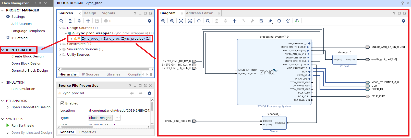
Open the base overlay that we used to compile Petalinux. If you lost it or need a working project you can just use this one.
Warning: this Vivado project is specifically built for my crystal-less EBAZ4205 and might not be suitable for other variants of the board.
Improtant: when loading an overlay PYNQ reprograms the hardware bitstream. Since EBAZ4205 has its network interface wired through PL lines and not the PS, make sure that you don't change the ethernet clock or pins for the overlay or ethernet will not work.
Save the base design as a new project with a dedicated name.
Open the Block diagram.
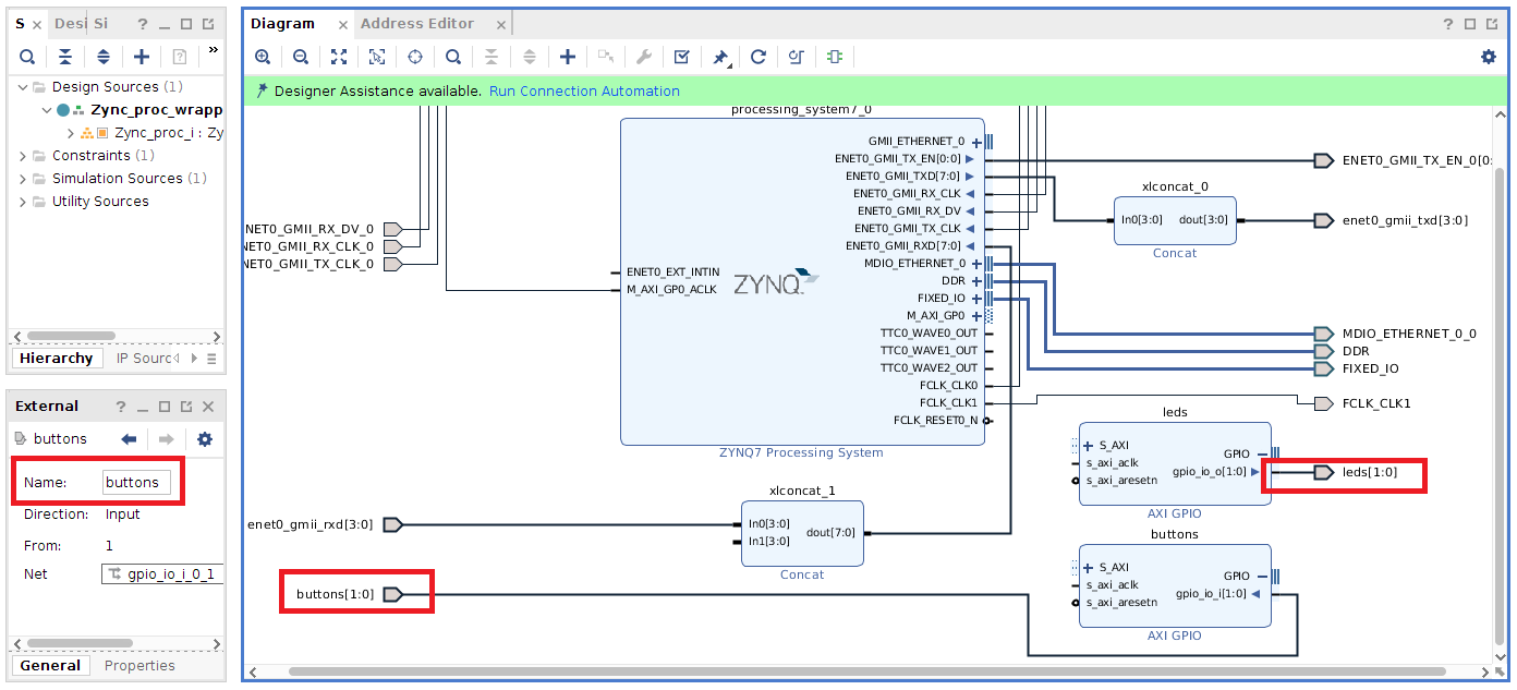
Double-click, define it with length of 2, outputs only.
Add another AXI GPIO to read the online buttons value, set it as length 2 input only (remember, these will NOT be routed from the onboard buttons)
Click "Run connection automation" and select the AXI interface to finalize module connection.
4. Add a custom Verilog hardware module: I will create here a simple even-number clock divider. AXI interface to PS can be done "properly" by creating hardware IPs. However, I figured a simplified way to achieve the same goal with GUI-only design by "hacking" the AXI-GPIO module. My method is not memory efficient (AXI module address size is minimum 4kB) and may have other issues that I am unaware of, but is very straightforward and worked for me so far. You are welcome to use either method you'd like.
A simple Verilog frequency divider code.
module clk_div(
//cell clocking
input clk_in,
input rst,
input [7:0] clk_div, //divide from 2 to 256, by even numbers only.
output reg clk_out
);
reg[7:0] counter=8'd0;
// clk_out = clk_in/clk_div
always @(posedge clk_in)
begin
if (rst==1'b0)
begin
clk_out <= 1'b0;
counter <= 8'd0;
end
else
begin
counter <= counter + 8'd1;
if(counter>=(clk_div-1)) counter <= 8'd0;
clk_out <= (counter<clk_div/2)?1'b1:1'b0;
end
end
endmodule
Create a new design source.
Name the module, finish (click OK without adding IOs. "Yes" when notified that module definitions have not changed).
Double click the new Verilog file and Add divider code. Save.
Double click the block diagram. Drag-drop the divider to block diagram to create a design block.
Add AXI-GPIO cells to interface the custom hardware. We will use a 32-bit output line, even though this is not strictly required in order to show how to split output bits.
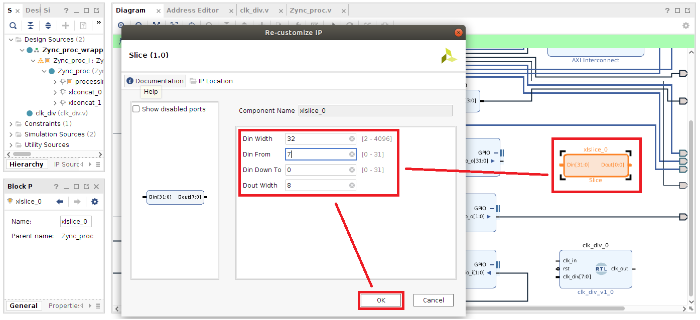
Add slice blocks to select the bits that control the different clock definitions. Since we have a single field here it is not strictly required, but if you want to interface many inputs with a single AXI register it's very convenient.
Edit the slice to output only 8 bits, rename to say what they are
Connect the divider input lines, make external port, and connect the AXI GPIO to the divider via the slice block. Note how the divider clock is connected to the Zynq master clock. This is not mandatory. If you want another base frequency you can add another PL clock to the Zynq block.
Finally, run block connection automation and connect the remaining AXI lines.
5. Add IOs to constraint files (pins are taken from the EBAZ4205 schematic).
We will route our input ("buttons") pins through the GPIO connector
This can be done Either
(a) Directly to constraint text file:
Add the following port allocation to your constraint file.
set_property IOSTANDARD LVCMOS33 [get_ports {buttons[1]}]
set_property IOSTANDARD LVCMOS33 [get_ports {buttons[0]}]
set_property IOSTANDARD LVCMOS33 [get_ports {leds[1]}]
set_property IOSTANDARD LVCMOS33 [get_ports {leds[0]}]
set_property IOSTANDARD LVCMOS33 [get_ports clk_out]
set_property PACKAGE_PIN W13 [get_ports {leds[1]}]
set_property PACKAGE_PIN W14 [get_ports {leds[0]}]
set_property PACKAGE_PIN A20 [get_ports clk_out]
set_property PACKAGE_PIN B19 [get_ports {buttons[1]}]
set_property PACKAGE_PIN B20 [get_ports {buttons[0]}]
Or
(b) By clicking "Run Synthesis", and then assigning pins via GUI:
Start by running synthesis. Confirm pin size mismatch warnings. These were by design.
If you cannot see an I/O ports tab at the bottom click Layout-> I/O Planning.
Assign the correct ports, directions and I/O standards to our required pins.
Save constraints to file (This will invalidate your synthesis).6. Run "Generate Bitstream" and gather required files.
Confirm rerun synthesis, select all CPUs
Open the block diagram and export the block design .tcl
find and copy the following files from your projects to a sperate location and rename them all as you desired overlay.
(a) .tcl file in wherever you saved it (default project base directory).
~/Vivado/2019.1/EBAZ4205_Ex_Overlay/Zynq_proc.tcl
(b) .bit file in the run implementation file
~/Vivado/2019.1/EBAZ4205_Ex_Overlay/EBAZ4205_Ex_Overlay.runs/impl_1/Zynq_proc.hwh
(c) .hwh file in the hardware wrapper handoff directory.
~/Vivado/2019.1/EBAZ4205_Ex_Overlay/EBAZ4205_Ex_Overlay.srcs/sources_1/bd/Zync_proc/hw_handoff/Zynq_proc_wrapper.bit
It is highly recommended that you change your PYNQ hostname if you use it on a multi-user network (e.g. university). Then, rename these three files to have the same name and upload to PYNQ.
If all went well, you should have a functional overlay!
If had trouble along the way or unsure of your design, I'm attaching mine here for your convenience.
7. Examine the uploaded overlay.
Make a python 3 file in the same directory as the uploaded overlay files. double click to open the file.
Import overlay content (I use screenshots and not a text box here to show how GUI functions).
Test LEDs functionality.
Test Variable clock (Oscilloscope/logic analyzer needed).
Since we don't have physical buttons, I will connect either 0V or 3.3V taken from serial port VCC to one of the "button" inputs.
WARNING! FPGA ports are much less forgiving than Arduino, for example. If you connect higher voltage than defined they are likely to burn.
And... done!
With custom logic, the sky is the limit. I hope that this little taste of PYNQ capabilities will drive you to move forward to much more complicated implementations. Happy hacking!


Comments
Post a Comment